The question worth asking
Does the answer still change when you refine?
Resolution is an input, not a result, and no single run can tell you whether the one you picked was fine enough. The question worth asking is the one you can actually check: does the answer still change when you refine? On the package below, it does not — which means a resolution you can afford already carries the answer a far finer one would give.
The case — a production-class accelerator package
The package
AMD MI350-class · 8 compute dies, 2 I/O dies, 8 HBM3E stacks
| Package | 64 × 72 mm |
| Silicon interposer | 54 × 62 mm |
| Mechanical layers | 457 |
| Footprint regions | 273 |
| Modelled instances | 138 |
| Material entries | 140 |
| Stack height | 1327 µm |
| Thermal load | 200 → 85 °C |
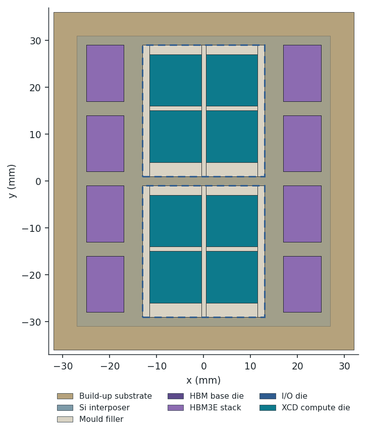
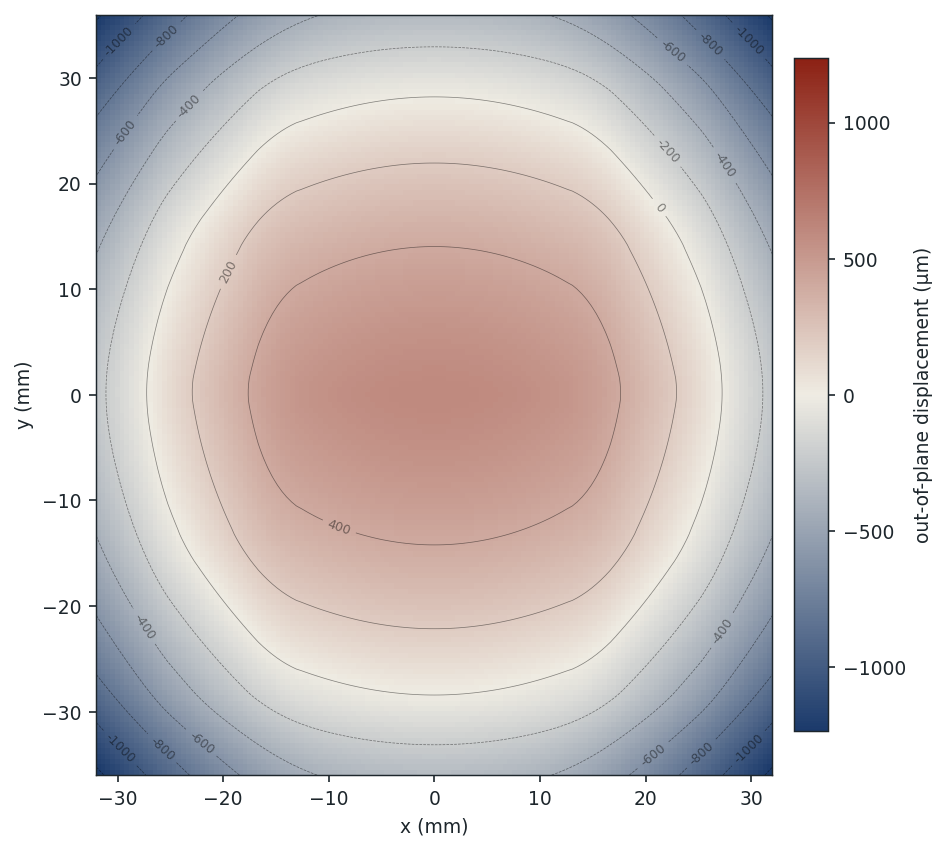
Imported from a 3Dblox description and solved as a 3D solid, layer by layer, through the full thickness of the stack — no plate approximation and no smeared effective stiffness. Eight XCD compute dies, two I/O dies and eight twelve-high HBM3E stacks, cooled from assembly to operating temperature.
The warpage
Active surface · assembly to operating temperature
The same answer at three resolutions
Refine it and watch
Three resolutions spanning a 2.25× range
| Resolution | Degrees of freedom | Peak-to-peak |
|---|---|---|
| 1143 µm | 351,222 | 1828.0 µm |
| 758 µm | 703,230 | 1830.6 µm |
| 507 µm | 1,427,412 | 1834.0 µm |
| Spread across all three | 4.1× the DOF | 6.0 µm · 0.33% |
Four times the degrees of freedom moves the answer by six microns on a package that bows by eighteen hundred. Counting everything — the spread above, the surface-by-surface agreement beside it, and the solver's own tolerances — total numerical uncertainty on this result is ±0.55%.
Not just the headline number
The whole surface, point by point
| Peak-to-peak warpage | 1834.0 µm |
| Corners | −1236.1 µm |
| Centre | +597.9 µm |
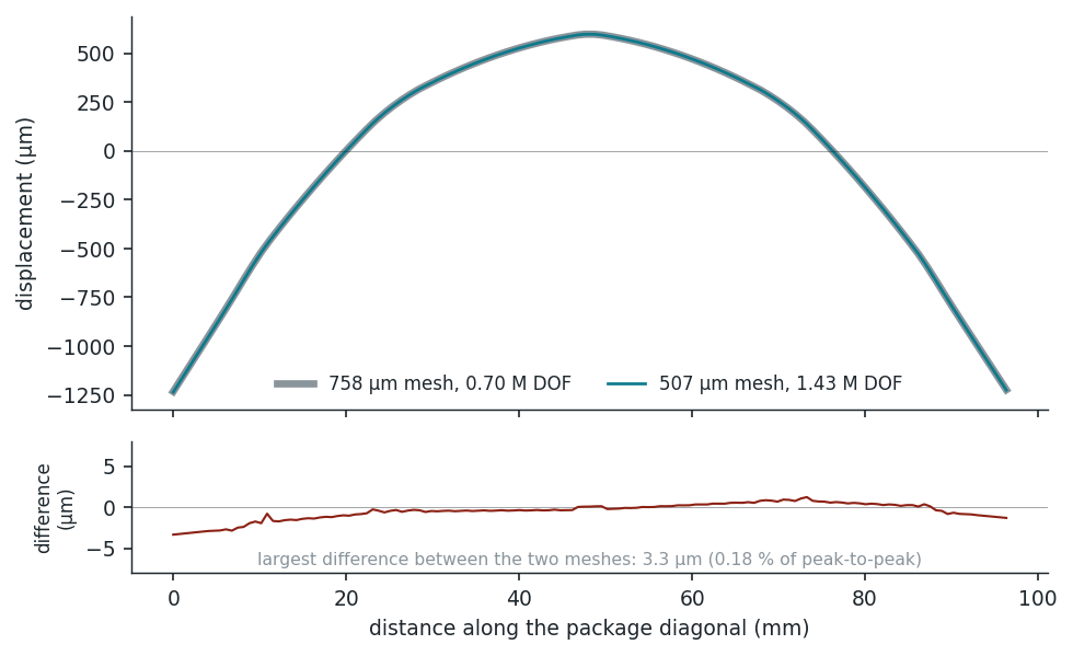
| Largest point-by-point difference | 3.3 µm · 0.18% |
| Total numerical uncertainty | ±0.55% |
A single peak-to-peak number could agree between two resolutions by coincidence. This is the whole field compared point by point along the package diagonal — the largest disagreement anywhere on the surface is 3.3 µm, less than a fifth of one percent of the bow.
Two resolutions, drawn on top of each other
Displacement along the package diagonal · 0.70 M and 1.43 M degrees of freedom
What the finer mesh would have cost
What this run cost
The reported result, end to end
| Resolution | 507 µm |
| Degrees of freedom | 1.43 M |
| Peak memory | 12.5 GB |
| Solve time | 11 min |
| Hardware | Apple M3 laptop |
Eight cores and 24 GB — a laptop, not a cluster. All three resolutions together cost under an hour.
What 50 µm would cost
Projected from the structure of the mesh — not solved
| Resolution | Degrees of freedom | Memory |
|---|---|---|
| 338 µm | 2.7 M | 23 GB |
| 225 µm | 5.7 M | 50 GB |
| 150 µm | 12.4 M | 109 GB |
| 100 µm | 27.2 M | 239 GB |
| 67 µm | 60.2 M | 530 GB |
| 50 µm | 107 M | ≈0.9 TB |
A 50 µm mesh on this package is 75× the degrees of freedom of the run above and needs roughly 0.9 TB of memory; solve time scales at least with degrees of freedom, putting it on the order of a day. These rows are projections, not results — none of them was solved, because the evidence above says the answer they would return is already in hand.
What this buys you
Explore coarse, commit fine. Because the answer has stopped moving well above the resolution you were told to ask for, early design work can run at a resolution that costs minutes on a laptop instead of a day on a machine you would have to buy. You spend the fine-resolution budget once, late, on the localized region that actually needs it — rather than paying it on every candidate in a sweep.
minutes, not days
a laptop, not a cluster
±0.55% total numerical uncertainty
the whole field, not just peak-to-peak
Scope of this study. The model is a free package body: the board, the BGA layer, the lid and any stiffener are excluded, and it includes no moisture, no cure shrinkage and no gravity. Each of those stiffens a real assembly and reduces warpage. Material properties are library values for the material classes involved, not vendor data. Production parts of this class measure substantially lower; the 1834.0 µm above is a property of the model as specified and is not a prediction of shipping hardware. What transfers to your design is the method and its cost — the agreement across resolutions, and the price of the mesh you were about to pay for. AMD, Instinct and MI350 are trademarks of Advanced Micro Devices, Inc. NoveetyAI is not affiliated with, endorsed by, or sponsored by AMD, and this study was not produced in cooperation with AMD.