A what-if, resolved
Microseconds per design point, with a bound attached
The compact model is built over a bounded box around a nominal design — by default ±10% on each material property — and inside that box every answer carries a rigorous error bound with it. Ask for a point outside the box and it still answers, still reports its bound, and tells you that you have left the region it was built for. Change the floorplan and it refuses to load at all.
The nominal design, before any what-if
2nm CoWoS · 8 HBM stacks, 2 GPUs, 108 chiplets · active surface
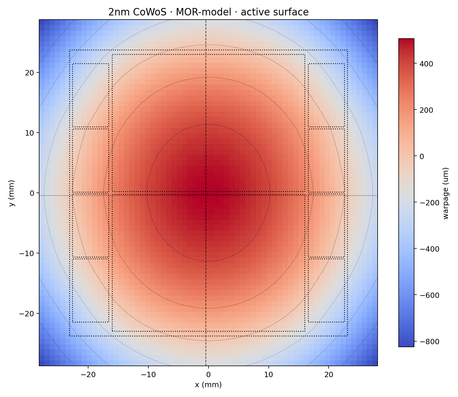
A what-if the model was never built at
ABF substrate stiffened 24.0 → 28.8 GPa
The WarpStack-MOR is a physics-based compact model built once per design from the same 3D formulation — not a black-box fit to data. Here the substrate is stiffened, a change that moves peak-to-peak warpage by +40.9 µm. The WarpStack-MOR resolves that shift to within 0.036 µm — in 51 µs rather than 40.6 s.
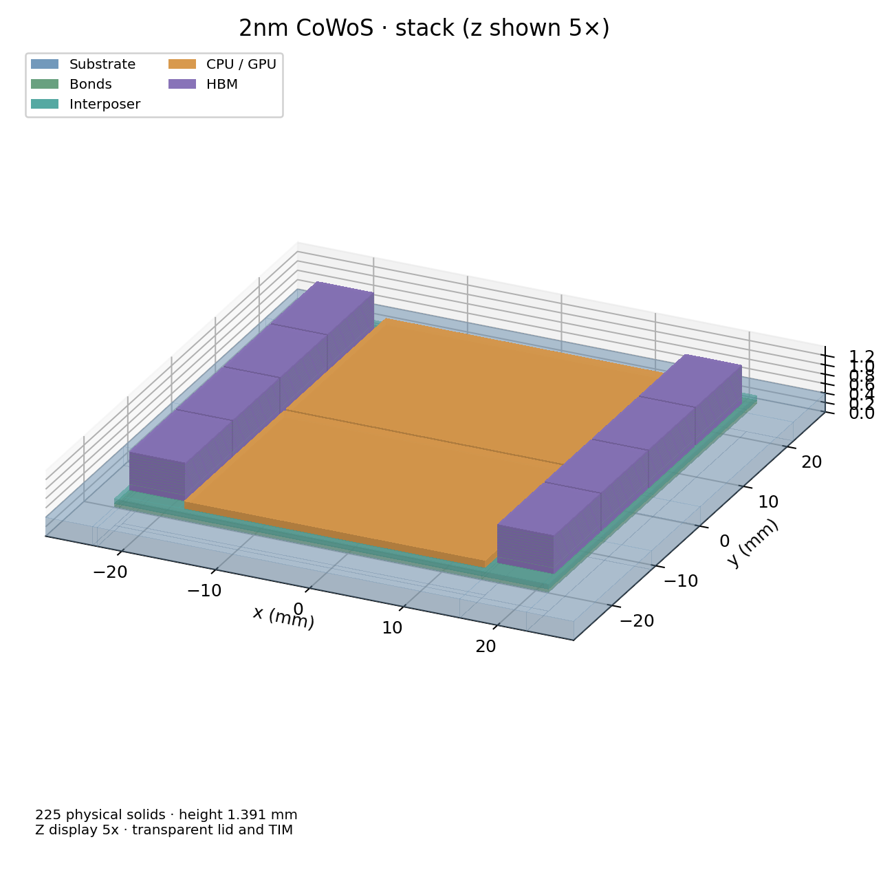
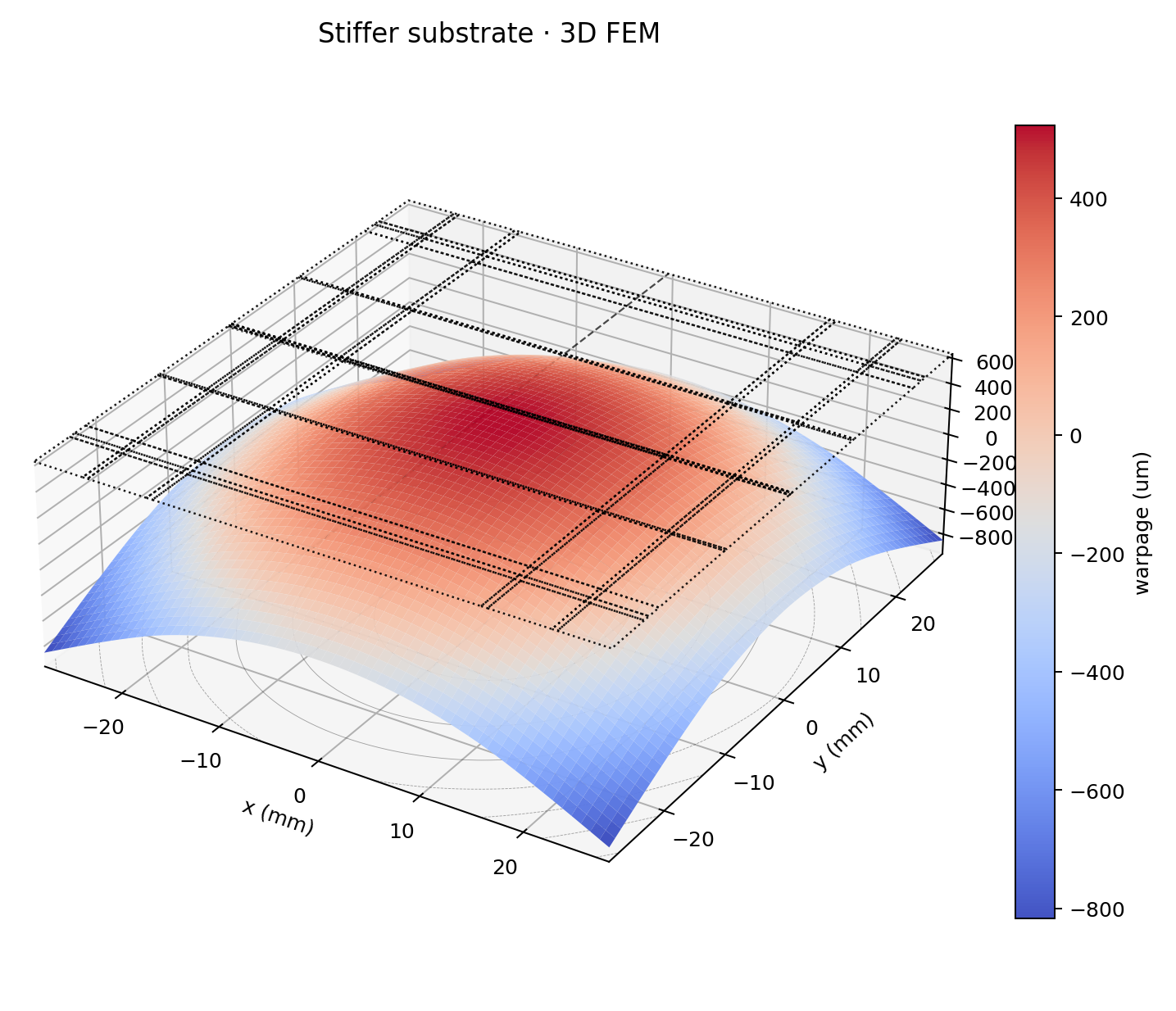
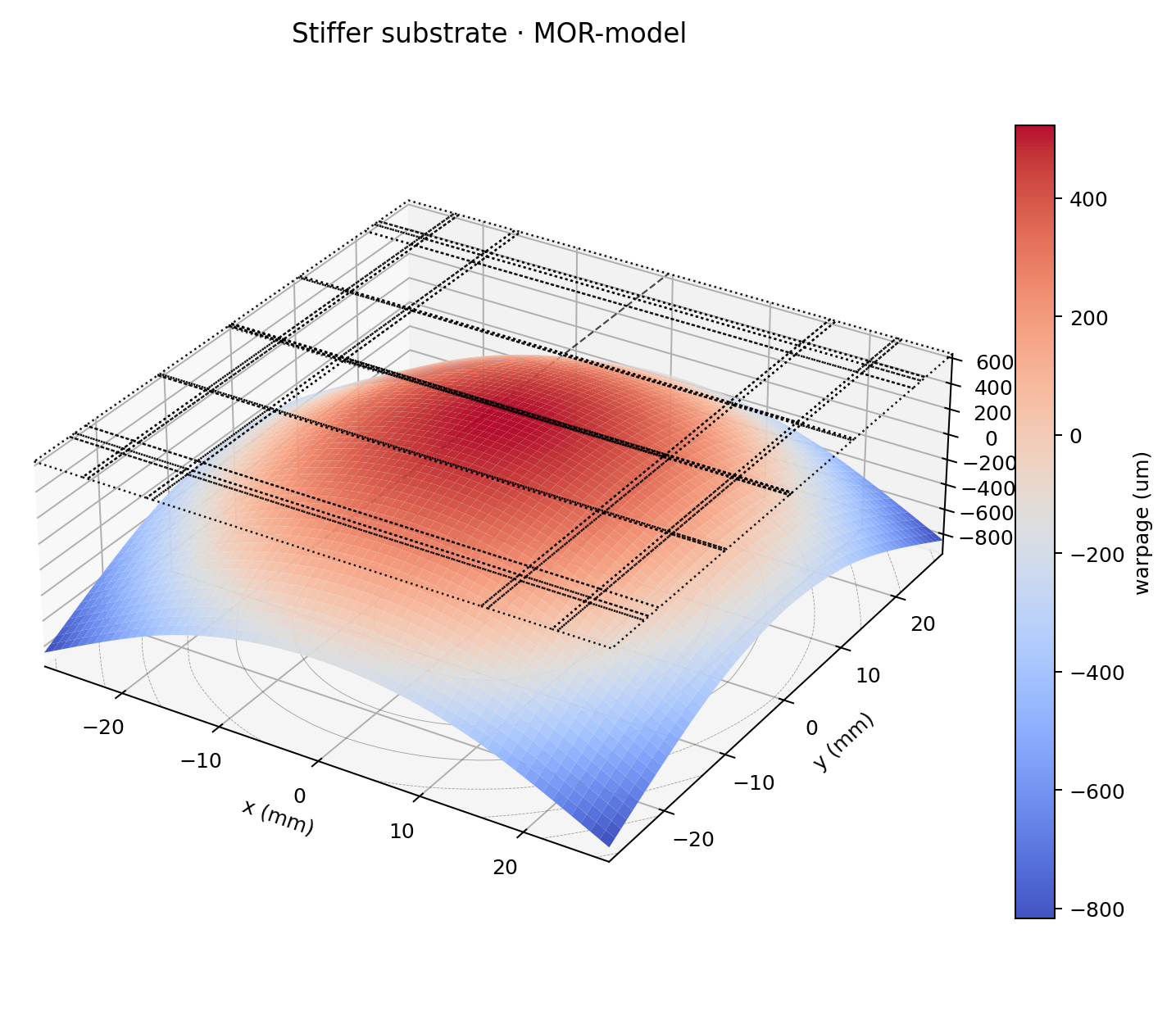
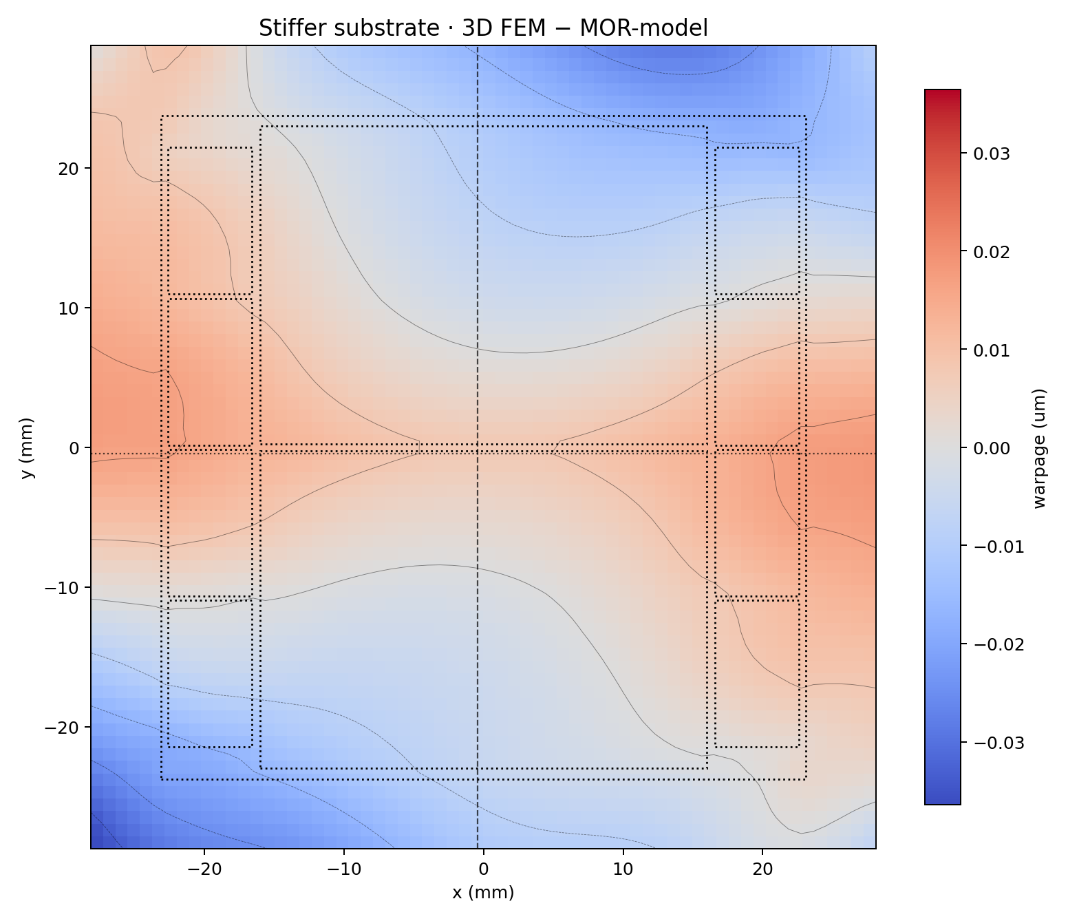
Both maps are the active surface at the same mesh and the same thermal load, so this compares the two methods like for like rather than against measurement. On this package the active and continuous package surfaces agree to within 0.1% of peak-to-peak — the bow is global, so the die-level and package-level views coincide.
How closely WarpStack-MOR tracks 3D
Stiffened-substrate what-if · same mesh, same load
| Quantity | Full 3D solve | WarpStack-MOR |
|---|---|---|
| Peak-to-peak warpage | 1372.7 µm | 1372.6 µm |
| Time per design point | 40.6 s | 51 µs |
| Peak-to-peak difference | reference | 0.043 µm |
| Whole-map difference | — | 0.003% |
| Largest local difference | — | 0.036 µm |
This point was deliberately chosen outside the set the model was built from. A further 8 design points drawn from across the material design space were each solved with a full 3D solve and compared: worst whole-map difference 0.006%.
What that buys you
Design points per hour, single core
Building WarpStack-MOR for this design costs 17 min of 3D solves up front — about 25× a single 3D run — after which each additional design point is 51 µs. The investment pays for itself within roughly 25 evaluations, and everything past that is effectively free. That is what turns warpage from a sign-off check into something you sweep.
Read these numbers for speed and for agreement, not for absolute warpage. Mechanical properties for this reference design are illustrative values for the material classes involved, not calibrated 2nm, HBM4 or CoWoS process data, and its peak-to-peak figures are quoted at a fixed resolution rather than settled against refinement. The timings, the speedup, and the agreement between the 3D reference and WarpStack-MOR do not depend on either. For warpage that has been checked across resolutions, see white paper No. 01.